SEMICONDUCTOR MANUFACTURING
- Duration: Sep. 2013 - Mar. 2019 (5.5 years)
- Taiwan Semiconductor Manufacturing Company
- Position: Senior R&D Module Engineer
In charge of 10nm & 5nm Back End of Line etching process
development.
- Leading a cross module project with 10 people. Save 50%
process time and invent a system for early stage validation,
which saving 50% resources.
- Product yield increase from 0% to 90%.
- 50% cost reduction by recipe optimization.
- Leading a cross module project with 10 people. Save 50%
process time and invent a system for early stage validation,
which saving 50% resources.
- Product yield increase from 0% to 90%.
- 50% cost reduction by recipe optimization.
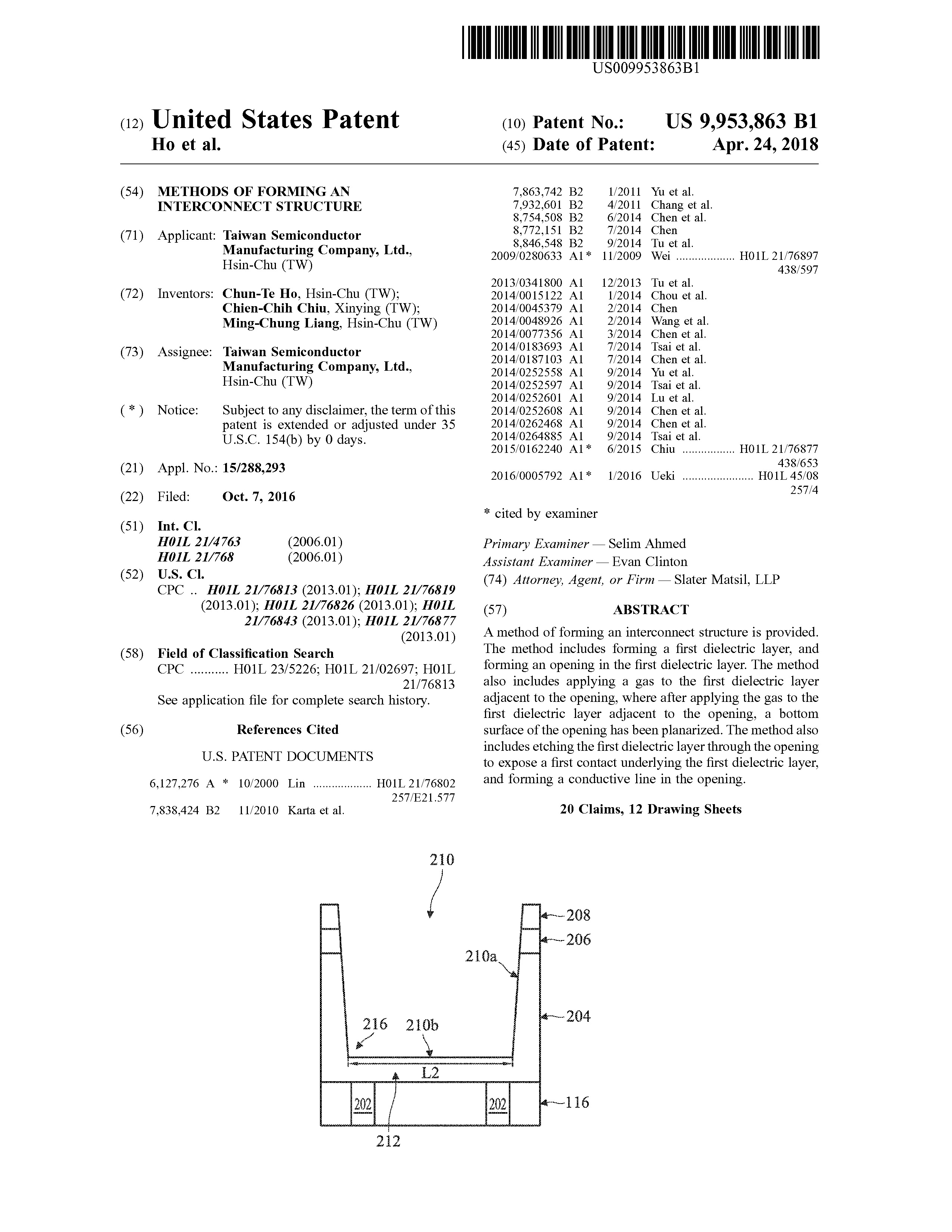
Methods of forming an interconnect structure
Chun-Te Ho , Chien-Chih Chiu, Ming-Chung Liang
US9953863B1
A method of forming an interconnect structure is provided. The method includes forming a first dielectric layer, and forming an opening in the first dielectric layer. The method also includes applying a gas to the first dielectric layer adjacent to the opening, where after applying the gas to the first dielectric layer adjacent to the opening, a bottom surface of the opening has been planarized. The method also includes etching the first dielectric layer through the opening to expose a first contact underlying the first dielectric layer, and forming a conductive line in the opening.

Integrated circuit fabrication with a passivation agent
Chun-Te Ho, Shih-Yu Chang, Da-Wei Lin, Chien-Chih Chiu, Ming-Chung LiangUS10290535B1
Examples of fabricating an integrated circuit device are disclosed herein. In an embodiment, an integrated circuit workpiece is received that includes a conductive interconnect feature. A first Inter-Level Dielectric (ILD) layer is formed on the conductive interconnect feature, and a second ILD layer is formed on the first ILD layer. A hard mask is formed on the second ILD layer. A via recess is etched extending through the first ILD layer, the second ILD layer and the hard mask to expose the conductive interconnect feature. The etching includes providing a passivation agent that reacts with a material of the hard mask to reduce etchant sensitivity.

Interconnect structure with vias extending through multiple dielectric layers
Chun-Te Ho, Ming-Chung Liang, Chien-Chih Chiu, Chien-Han ChenUS11251127
An embodiment includes a method. The method includes: forming a first conductive line over a substrate; depositing a first dielectric layer over the first conductive line; depositing a second dielectric layer over the first dielectric layer, the second dielectric layer including a different dielectric material than the first dielectric layer; patterning a via opening in the first dielectric layer and the second dielectric layer, where the first dielectric layer is patterned using first etching process parameters, and the second dielectric layer is patterned using the first etching process parameters; patterning a trench opening in the second dielectric layer; depositing a diffusion barrier layer over a bottom and along sidewalls of the via opening, and over a bottom and along sidewalls of the trench opening; and filling the via opening and the trench opening with a conductive material.